Summary of common level switching circuits
Time:2024-04-03
Views:196
I. Introduction
In the circuit designed by us, the pins of different chips use different voltages, such as common 1.8V, 3.3V, 5V, etc. We need to communicate devices with different communication levels, so we need to use level conversion for level matching. This paper introduces common level conversion methods.
2. Second, diode level conversion
Typical application: pull-up resistor and diode scheme
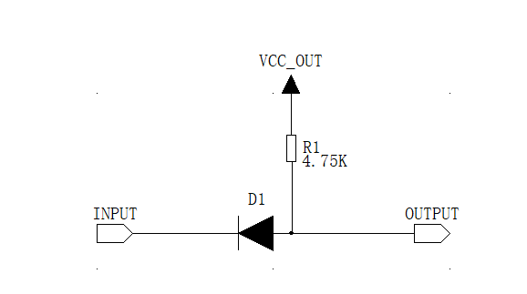
Figure 1 Diode conversion circuit
• Applicable scope: The input signal level is greater than the output signal conversion circuit• Advantages: Low cost, fewer components used
• Disadvantages: only one-way transmission, and the input signal level is greater than the output signal, the diode will produce a large voltage drop
The selection of the diode here should try to choose the Schottky diode with low voltage drop to ensure that the signal transmission will not cause the level reading error because the voltage drop of the diode is too large.
Working process analysis:
When the 3.3V device outputs a high level signal, the signal input device is pulled up to a 5V level due to the pull-up 5V action.
When the 3.3V device outputs a low level signal, the OUTPUT signal is pulled down, and the signal input device signal is pulled down.3. Three, transistor level conversion
The basic applications of triode circuits are as follows:
The basic applications of triode circuits are as follows:
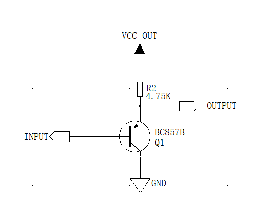
Figure 2 Triode conversion circuit
• Applicable scope: The input signal level is greater than the output signal conversion circuit
• Advantages: Low cost, fewer components used, compared with the diode, the triode signal input can be driven with a smaller current, which may be more advantageous in the case of some peripheral drive capacity is weak
• Disadvantages: only one-way transmission, and the input signal level is greater than the output signal
The range of action and advantages and disadvantages are similar to the diode circuit, the transistor will also produce a certain pressure drop because of the PN junction, so in the selection of the transistor, you can choose a lower on-voltage drop triode.
Working process analysis:
• When the 3.3V device outputs a high level signal, the signal input device is pulled up to a 5V level due to the 5V pull-up action.
• When the 3.3V device outputs a low level signal, the PNP diode is on and the signal input device signal is pulled down.
4. Four, MOS level conversion:
• Scope of application: Suitable for most application scenarios requiring level conversion
• Advantages: two-way transmission, the on-voltage drop is generally small, and the transmission frequency can reach a high level
The following is a working process analysis of one of I2C‘s signal lines:
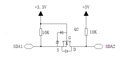
FIG. 3 MOS tube conversion circuit
When SDA1 output high voltage: MOS tube Q1 Vgs = 0, MOS tube off, SDA2 is pulled up to 5V by resistor R3.
When SDA1 output low voltage: MOS tube Q1 Vgs = 3.3V, greater than the on-voltage, MOS tube on, SDA2 through the MOS tube is pulled to low level.
When SDA2 outputs high voltage: the Vgs of MOS tube Q1 is unchanged, MOS remains off, and SDA1 is pulled up to 3.3V by resistance R2.
When the SDA2 output low voltage: the MOS tube is not on, but it has a body diode, the body diode in the MOS tube pulls the SDA1 down to the low level, at this time Vgs is about 3.3V, the MOS tube is on, further pulling down the voltage of SDA1.
5. Five, level conversion chip
If the signal conversion frequency requirements are high, and do not want to produce a large voltage drop, many manufacturers have designed a special level conversion chip.
The following is the introduction of a factory level conversion chip, the chip characteristics are as follows:
• Wide level switching range: VCC(A): 1.65V to 3.6V and VCC(B): 2.3V to 5.5V
• Maximum data rate: 50 Mbps
• Multiple packages
• Number of conversion channels: 4
• Mainly applicable to: I2C, UART, GPIO, etc
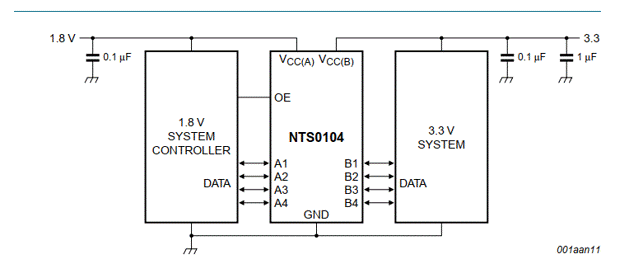
Figure 4 Typical application of NTS0104
6. Vi. Conclusion
There are many ways and circuits of level conversion, and the appropriate scheme can be selected according to the actual needs. At present, the level conversion chip has been very mature, and it is recommended to choose the level conversion chip will be more suitable for most cases.
When SDA1 output low voltage: MOS tube Q1 Vgs = 3.3V, greater than the on-voltage, MOS tube on, SDA2 through the MOS tube is pulled to low level.
When SDA2 outputs high voltage: the Vgs of MOS tube Q1 is unchanged, MOS remains off, and SDA1 is pulled up to 3.3V by resistance R2.
When the SDA2 output low voltage: the MOS tube is not on, but it has a body diode, the body diode in the MOS tube pulls the SDA1 down to the low level, at this time Vgs is about 3.3V, the MOS tube is on, further pulling down the voltage of SDA1.
5. Five, level conversion chip
If the signal conversion frequency requirements are high, and do not want to produce a large voltage drop, many manufacturers have designed a special level conversion chip.
The following is the introduction of a factory level conversion chip, the chip characteristics are as follows:
• Wide level switching range: VCC(A): 1.65V to 3.6V and VCC(B): 2.3V to 5.5V
• Maximum data rate: 50 Mbps
• Multiple packages
• Number of conversion channels: 4
• Mainly applicable to: I2C, UART, GPIO, etc

Figure 4 Typical application of NTS0104
6. Vi. Conclusion
There are many ways and circuits of level conversion, and the appropriate scheme can be selected according to the actual needs. At present, the level conversion chip has been very mature, and it is recommended to choose the level conversion chip will be more suitable for most cases.
|
Disclaimer: This article is transferred from other platforms and does not represent the views and positions of this site. If there is any infringement or objection, please contact us to delete it. thank you! |


