LED control method for I2C in LED driver
Time:2023-06-10
Views:975
The power supply is an important part of the entire circuit board, and it is unstable. Don‘t talk about anything else.
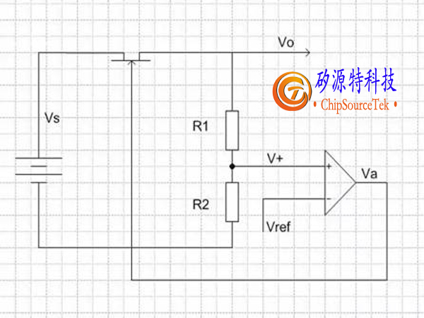
In power supply design, we often use a stable "high" voltage to obtain a stable "low" voltage. This is also commonly referred to as DC/DC, where there are two types of power regulator chips that are commonly used. One is called LDO (low voltage differential linear regulator, which we will refer to later as a linear regulator power supply), and the other is called PWM (pulse width modulation switching power supply, which we will also refer to as a switching power supply in this article). We often hear about the high efficiency of PWM, but the fast response of LDO. Why is this? Don‘t worry, let‘s take a look at their principles first.
The following will involve some theoretical knowledge, but it is still very simple and easy to understand. If you don‘t understand, hehe, you need to check your foundation.
1. The working principle of linear regulated power supply

2. Working principle of switching power supply

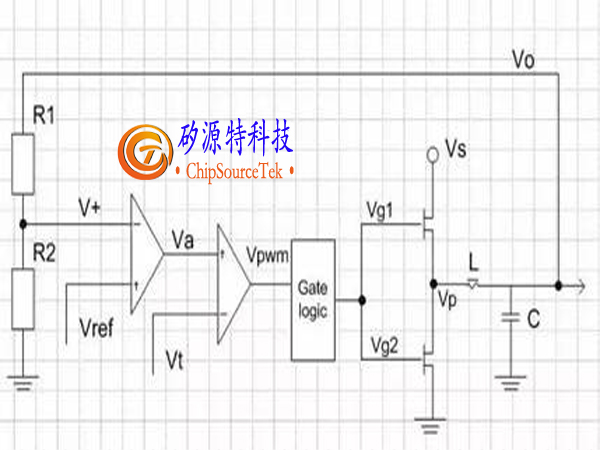
As shown in the above figure, in order to obtain Vo from high voltage Vs, the switching power supply uses a square wave Vg1 with a certain duty cycle, where Vg2 pushes the upper and lower MOS transistors. Vg1 and Vg2 are in reverse phase, with Vg1 being high and Vg2 being low; When the upper MOS tube is opened, the lower MOS tube is closed; When the lower MOS tube is opened, the upper MOS tube is closed. As a result, a square wave voltage with a certain duty cycle is formed at the left end of L, and the inductance L and capacitor C can be regarded as low-pass filters. Therefore, the square wave voltage is filtered to obtain a stable voltage Vo after filtering. After being divided by R1 and R2, Vo is sent to the negative terminal V+of an amplifier (error amplifier). The output Va of the error amplifier serves as the positive terminal of the second amplifier (PWM amplifier). The output VPWM of the PWM amplifier is a square wave with a certain duty cycle, which is processed by the gate logic circuit to obtain two inverted square waves Vg1 and Vg2 to control the switching of the MOSFET.
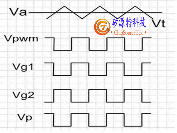
The positive end Vref of the error amplifier is a constant voltage, while the negative end Vt of the PWM amplifier is a triangular wave signal. Once Va is greater than the triangular wave, VPWM is high; When Va is smaller than the triangular wave, VPWM is lower. Therefore, the relationship between Va and the triangular wave determines the duty cycle of the square wave signal VPWM; When Va is high, the duty cycle is low, and when Va is low, the duty cycle is high. After processing, Vg1 is in phase with VPWM, while Vg2 is in phase with VPWM; The square wave voltage Vp at the left end of terminal L is the same as Vg1. As shown in the following figure

When Vo rises, V+will rise, Va will decrease, and VPWM duty cycle will decrease. After logical analysis, the duty cycle of Vg1 will decrease, the duty cycle of Vg2 will increase, and Vp duty cycle will decrease. This in turn leads to a decrease in Vo, and the rise of Vo will be suppressed. The reverse is also true.
3. Comparison between linear regulated power supply and switching power supply
After understanding the working principles of linear regulated power supplies and switching power supplies, we can understand why linear regulated power supplies have low noise, fast transient response, but poor efficiency; The switching power supply has high noise, slow transient response, but high efficiency.
The internal structure of a linear regulated power supply is simple, with a short feedback loop, resulting in low noise and fast transient response (compensation is fast when the output voltage changes). However, due to the fact that the pressure difference between input and output is entirely distributed on the MOSFET, its efficiency is low. Therefore, linear voltage regulation is generally used in applications with low current and high voltage accuracy requirements.
The switching power supply has a complex internal structure and many factors that affect the output voltage noise performance. Moreover, its feedback loop is long, so its noise performance is lower than that of linear regulated power supply and its transient response is slow. However, according to the structure of the switching power supply, MOSFETs are in two states: fully open and fully closed. Except for the energy consumed by driving MOSFETs and MOSFET‘s own internal resistance, all other energy is used for output (theoretically, L and C do not consume energy, although this is not the case in practice, the energy consumed is very small).
|
Disclaimer: This article is transferred from other platforms and does not represent the views and positions of this site. If there is any infringement or objection, please contact us to delete it. thank you! |


