A little neglect can ruin EMI performance
Time:2022-12-03
Views:1504
It is easy to find 100fF capacitors as parasitic components in the power supply. Therefore, it must be understood that only by properly handling them can we obtain power supply that meets EMI standards.
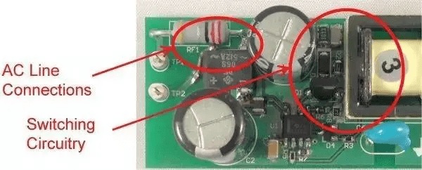

A small amount of parasitic capacitance (100 millimicrofarad) from the switch node to the input leads can prevent you from meeting your electromagnetic interference (EMI) requirements. What does a 100fF capacitor look like? In Digi Key, there are few such capacitors. Even if they do, they provide broad tolerances due to parasitic problems. However, it is easy to find 100fF capacitors as parasitic components in your power supply. Only by properly handling them can we obtain power supply that meets EMI standards. Figure 1 is an example of these unplanned capacitors. On the right side of the figure is a vertically mounted FET with switch nodes and clamping circuits extending to the top of the picture.
The input connection enters from the left to the position within 1cm from the drain connection. This is the fault point, where the switching voltage waveform of FET can bypass the EMI filter and be coupled to the input.

Fig. 1 Proximity of switch node and input connection will reduce EMI performance
Note that there is some shielding provided by the input capacitor between the drain connection and the input lead.
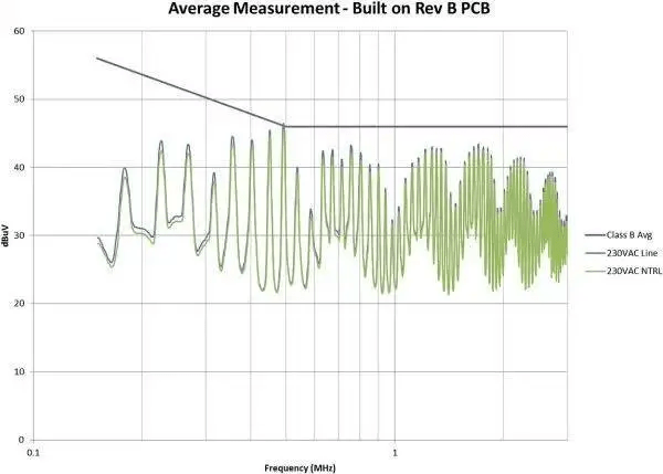
The case of the capacitor is connected to the main ground, which provides a path for common mode current to return to the main ground. As shown in Figure 2, this tiny capacitance will cause the power EMI signature to exceed the specification.

Figure 2 EMI Performance Exceeding the Specification Requirements Caused by Parasitic Drain Capacitance
This is an interesting curve, because it reflects several problems: lower frequency radiation that obviously exceeds the specification requirements, 1MHz to 2MHz components with common mode problems that are usually obvious, and attenuation sine (x)/x distribution of higher frequency components. Measures need to be taken to keep the radiation within the specification. We use the general capacitance formula to reduce it:
C = ε ˙ A/d
We can‘t change the permittivity( ε), And the area (A) is already the smallest. However, we can change the spacing (d). As shown in Figure 3, we extended the distance between the component and the input by three times. Finally, we use a larger ground plane to increase shielding.

Figure 3 The modified layout can not only increase the spacing, but also bring shielding performance
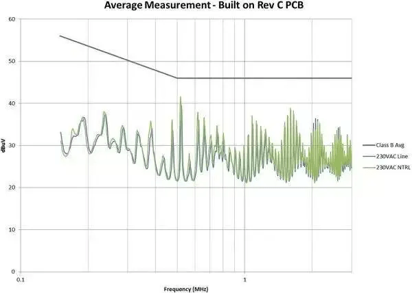
Figure 4 is the modified rendering. We have obtained a margin of about 6dB for the EMI specification at the point of failure.
In addition, we have significantly reduced overall EMI signatures. All these improvements are only due to the adjustment of the layout, and do not change the circuit.
If your circuit has a high voltage switch and uses a shielding distance, you need to control it very carefully.

Figure 4 EMI performance improved through shielding and increased spacing
In conclusion, the 100fF capacitance from the switching node of the off-line switching power supply will cause EMI signatures that exceed the specification requirements. This capacitance can be easily realized by only parasitic components, such as routing drain connections close to input leads.
This problem can usually be solved by improving spacing or shielding. In order to obtain greater attenuation, it is necessary to increase filtering or slow down the circuit waveform.
|
Disclaimer: This article is transferred from other platforms and does not represent the views and positions of this site. If there is any infringement or objection, please contact us to delete it. thank you! |


