PCB High Speed Circuit Board Layout Design Guide
Time:2022-11-03
Views:1650
Key points of this article
• Prepare for high-speed PCB layout
• Device placement and PDN development in high-speed design
• Practical PCB high-speed wiring suggestions
In order to meet the needs of today‘s electronic products, the speed of digital circuits is becoming faster and faster. High speed design was once an unpopular field of electronic products, but now, most products need at least part of "high speed design". These designs require PCB designers to arrange PCB according to high-speed rules and requirements; For some designers, this is a new field. To this end, this article summarizes some of the most common high-speed PCB design guidelines, hoping to be helpful to your high-speed layout design.
Setup of high-speed design
Before starting layout design, there are many design and database details that need to be handled properly in advance.
schematic diagram
Although there are many contents to be set before starting to design high-speed PCB layout, most people do not consider the schematic too much. The designer should verify the components and simulation circuits and complete the design. But is the schematic itself ready for layout? If the designer cannot easily understand the intention of the circuit, the disordered schematic diagram will make PCB layout more difficult. For example, high-speed signal paths need to be placed in order so that designers can locate the simulator in layout. It is also helpful to mark the design areas that you want the layout team to understand clearly. These include:
• Key placement positions, and which side of the circuit board some components may need to be placed on.
• Prohibited wiring area around key components.
• High speed cabling information, including cabling topology, measurement length, and matching length.
• Differential pair and controlled impedance information.
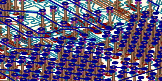
Dense wiring of high-speed circuit boards
PCB Library
Footprint used for high-speed design must be checked and verified like PCB layout, and some additional database work will also be involved. For example, in order to ensure signal integrity in high-frequency or RF designs, it may be necessary to modify the footprint used to reduce the pad size. In addition, some footprint may be reduced to the minimum size to meet the requirements of high-density design. However, the footprint of devices should follow the industry and manufacturer‘s specifications as much as possible to meet the requirements of design for manufacturability (DFM). Many design tools, such as Cadence Allegro PCB Editor, can provide online library browsing function, which is used to pull the footprint model of the specified supplier.
Materials and Devices
Before starting layout design, you must select the materials used to manufacture high-speed circuit boards. The harsh working environment may require a more robust circuit board structure, and the physical properties of materials are required to calculate the controlled impedance wiring:
• Communicate with the manufacturer to determine whether the circuit board needs high-speed materials.
• Reinforced epoxy or PTFE materials may be a better choice for high-speed and high-frequency applications.
• The dielectric constant of FR-4 may not be able to maintain the required impedance value, or cause a loss of signal beyond the acceptable range in the design.
• PCB components also need to be reviewed and confirmed by the manufacturer. In view of the current supply chain problems, it is necessary to ensure that components are available before starting the design.
Laminate stacking
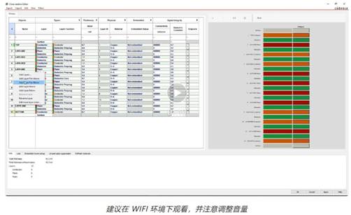
High speed design requires specific layer stacking to achieve EMI shielding and signal integrity. First of all, a complete and continuous grounding plane should be included in the internal layer. Many circuit boards also have multiple grounding plane layers on the entire circuit board stack for multi-layer transmission line wiring in microstrip line or stripline configurations. The layer stacking needs to be established in the PCB CAD database, and can also be imported from an external source. In this regard, it would be very helpful if the PCB design system could communicate directly with the supplier to exchange stacking information, as shown in the following video:

Design rules
PCB design systems usually have a very comprehensive set of design rules and constraints that can be set for design. Standard board designs use device and network classes to specify spacing rules, routing widths, vias, and other constraints. For high-speed design, a new set of rules should be set, including:
• Differential pair
• Signal path
• Cabling topology
• Measured and matched routing length
• Wiring adjustment parameters
You can set these rules for each design; Or, in many cases, import from another layout to reduce the workload of designers.
system parameter
The last item set is the parameter. Parameters are important, including display parameters such as color and fill patterns, grids, routing preferences, and a range of other parameters. By managing these parameters, designers can improve the efficiency of using tools.
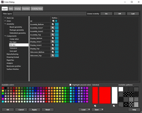

Parameter setting menu for color design in PCB CAD system
Now that we have completed the high-speed design setup, we can begin to lay out the circuit board.
PCB Design Guide for High Speed Device Placement
The placement of devices with high-speed design still needs to follow the same rules as the placement of standard design. For the sake of balance, the components shall be evenly distributed around the circuit board, and the manufacturing and test design rules (DFM and DFT) shall be followed. This includes the spacing between devices and other components, circuit board features, and circuit board edges. The devices operating at high temperature shall be concentrated to use the area on the circuit board as much as possible to dissipate heat, and attention must be paid not to obstruct the flow of air on the circuit board. Connectors and other human-computer interface components shall be placed in places easy to reach by technicians, and different power supplies shall be placed separately.
The difference of high-speed design is that it needs to achieve the best signal integrity in the whole design. A major part of signal integrity depends on a clear signal return path on the ground plane and on ensuring that digital and analog circuits are separated from each other. Therefore, in addition to supporting the required wiring, the device placement must also ensure clear signal return path and circuit isolation. In order to complete this kind of complex device placement, it is usually best to carry out layout planning before arranging the actual components on the circuit board. Layout planning helps to divide the functional partitions of circuits without constantly moving components.
As the partitions are determined one by one, it is time to place devices:
• High speed device placement guidelines
• Make room on the reference plane for clear signal return paths.
• Space cabling channels for dense data and memory bus cabling.
• Avoid placing components in areas where analog and digital circuits are interlaced.
• The components shall be placed in such a way that the high-speed signal path is short.
• The signal path can include multiple devices in the path, which should be placed according to the layout in the schematic diagram.
• Analog elements should be placed together as much as possible to reduce their routing length.
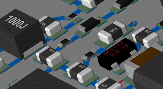


Placement of analog and power supply devices
As mentioned earlier, power distribution network (PDN) should be planned together with device placement plan. Next, let‘s learn some PDN design suggestions.
Power Distribution Network (PDN) Design
In high-speed circuit boards, carefully designed PDN is critical to the final electrical performance of the circuit board. If there is no clear signal return path, the circuit board may generate a lot of noise, which may lead to wrong signals and interfere with the normal operation of the circuit. It can also cause other signal integrity issues, such as EMI and ground bounce. The return signal of clear return path cannot be found on the reference plane, which may eventually be coupled to any return path they can find, including other routes. This unintentional coupling will generate common mode current, which may generate electromagnetic radiation and bring additional noise.
To avoid these problems, the following are some PDN design suggestions:
• Use a continuous ground plane, do not divide the ground plane
• Use device placement zoning to separate digital and analog circuits instead of dividing the ground plane.
• When wiring high-speed transmission lines, ensure that they have a clear signal return path on the adjacent ground plane. At higher speeds and frequencies, a return path will naturally form around the route, so it is easy to plan.
• Be careful with board features that may block the ground plane
• Too many vias, circuit board cuts or other obstacles in a concentrated area will destroy the clear return path on the reference plane.
• Avoid laying high-speed transmission lines where there are gaps adjacent to the ground plane.
High density device with large number of pins and multiple power connections
• Processors, memories and other high-density devices with large number of pins use many power supply pins to meet their huge power demand.
• In these connections, each connection requires a bypass capacitor as close to the power supply pin as possible to obtain the best power filtering effect.

High speed cabling example, you can see that the routing has been adjusted
Once the network connection and PDN of the circuit board are optimally configured, cabling can begin.
High speed wiring skills
When the components on the circuit board are properly arranged, the design will have a basic template to indicate how the wiring should be arranged. However, it should be noted that we will probably still have to move the components to improve and adjust the wiring - just like in any PCB design.
High speed cabling guidelines
• Ensure that the design rules and constraints for line length, matching length, width, spacing, layers, impedance controlled wiring parameters, differential pairs, routing adjustment, and via allocation are fully followed.
• Set up any necessary area rules according to the unique wiring requirements, and set aside prohibited wiring areas.
• In addition to the specific cabling topology and measurement length, try to make the cabling as short and direct as possible.
• Do not wire in the gap or disconnection of the grounding plane. This may damage the clear return path of the signal, and may cause the signal integrity problem discussed earlier.
• When wiring high-speed signals, ensure that they have a clear signal return path on the adjacent ground plane.
• For sensitive signals (such as clock lines and differential pairs), ensure that there is an additional gap between them and other wiring, usually three times the width of the standard wiring.
• Ensure that high-speed transmission lines are laid on their assigned layers to ensure their return paths on adjacent reference planes.
• Avoid changing the properties of layers through high-speed transmission lines, but if it is necessary to do so, try to make them adjacent to the same ground plane to obtain the signal return path. If the transition section of the layer is farther than the layer pair, a grounding via is used next to the signal via as the transition of the return path.
• High speed transmission lines that are parallel to each other should be treated with caution as they may cause crosstalk.
• Pay attention to the crosstalk in the vertical direction between layers, and the spacing may be smaller than the two parallel lines on the same layer.
• Use wider routing in analog cabling.
• Select a wider grid to place vias, and plan vias escape for the maximum number of routing channels.
• Minimize the use of vias to reduce inductance, or use blind holes, buried holes, or micropores.
• Be careful not to block the return path on the ground plane in areas with dense dispersed vias.
The design criteria of high-speed PCB listed in this paper are far from exhaustive, but they are enough to help us start to design high-speed PCB. In addition, remember to make full use of the functions of CAD tools. In addition to the design rules and constraints already mentioned above, Cadence PCB design tool has many other efficient functions to facilitate high-speed design, such as:
• Dynamic back drilling: back drilling information follows the design and is updated in real time. After design adjustment, there is no need to manually update the back drilling information.
• Micro hole inspection: set the design rules related to laser holes to ensure high quality delivery of HDI design.
• Parametric high-speed structure:
• The required high-speed structure can be generated by inputting parameters without tedious selection of high-speed structure elements;
• In design, high-speed structure is used just like vias (replacement, set in Constraint Manager).
• 3D Canvas: Let the designer see the PCB entity, and the assembled PCB is displayed in front of him.
• DFM/DFA design: different DFM/DFA rules are set for different areas.
• Allegro Constraint Compiler: convert design guidelines into design rules, realize the same source of rules, and help designers quickly and accurately reuse rules.
|
Disclaimer: This article is transferred from other platforms and does not represent the views and positions of this site. If there is any infringement or objection, please contact us to delete it. thank you! |


